Showing posts with label Semiconductor. Show all posts

Monday, June 8, 2015

Probing C and N doped titanium dioxide with hard x-ray photoelectron spectroscopy

Titanium dioxide (TiO2) is a widely used band-gap semiconductor with vast applications in photocatalysis, photovoltaic, and spintronics.    Recent advances by Japanese researchers has sparked interest in TiO2 for electro-photo-catalytic splitting of water, since this mineral is a widely used white pigment with UV absorbance characteristics.  The Achilles heal of this application is its large band-gap (3.20 and 3.00 eV for anatase and rutile crystal phases, respectively).  Hence the push toward doping for lower band-gap.  Among the several anionic dopants attempted, N was the most effective for lower band-gap and thus enhance photocatalysis under visible light.  This is made possible by the overlap of the N 2p orbitals with the O 2p orbitals with respect to the energy it would take for a photon to knock an electron out of those orbitals and into the so-called conduction band, where current can be generated.  This makes intuitive sense since N and O are neighbors on the periodic table.  Doping with N can be further enhanced with C.  Doping with only carbon is bad because its 2p orbitals do not overlap with the O 2p orbitals, which would create separate quantum levels for conducting electrons to occupy and not do anything.  However, the C 2p orbital overlaps with the N 2p orbital.  This means we'd have 2p orbitals from two dopant atoms overlap with the oxygen 2p, which gives engineers more flexibility in lowering the TiO2 band-gap.

Up to then, little data has been collected on these C- and N-doped TiO2. The paper by Ruzybayev et al attempts to fill those gaps.   Experimental data was acquired via hard x-rays from the National Synchrotron Light Source (NSLS)  in Brookhaven National Laboratory (now closed because NSLS II is opening now).  Hard x-rays have an energy range of 5-15 keV (about the same as medical x-rays), and penetrate into the sample bulk; soft x-rays range 1-5 keV and only penetrate the surface of a sample .  Both types of x-rays are useful, but it depends on the application.  This makes for an interesting paper because my master's thesis was a theoretical study of hard x-rays inducing photoemission from a magnetic multilayer structure.  The technique is known as hard x-ray photoelectron spectroscopy (HXPS).

The experimental section will be skipped for brevity, but the specimens were TiO2 films that were only 500 nm thick.  That's close to the wavelength of blue light.  The optical band-gap of pure TiO2 and co-doped TiO2 is shown in UV-Vis diffuse reflectance spectroscopy data on Figure 1.
Figure 1.  Approximated band-gaps for pure TiO2 and C and N doped TiO2.
Pure TiO2 has a band-gap of 3.30 eV, as evidenced by the upward slope of the solid curve in Figure 1.  Codoping lowered the band-gap to 2.39 eV, (deeply slanted slope of the dashed curve).  The analysis from HXPS data is displayed in Figure 2.  This can be considered the "meat" of the paper because it explicitly shows how the C and N dopants affect the electronic structure of TiO2.  "Electronic structure" has many contexts, but the important one here is the oxidation state of titanium.

Figure 2.  HXPS of titanium 2p orbital in pure form and doped with C and N.
The two peaks in the pure TiO2 spectrum show the characteristic 2p3/2 and 2p1/2 spin-orbit split of Ti4+ (marked A and B in the upper curve, respectively).  The superscript 4+ represents its oxidation state, i.e., the charge experienced by the titanium atom after giving away four electrons to two oxygen atoms (each oxygen atom having two additional electrons).  Doping induced two additional peaks adjacent to the the orbitals.  The 'C' and 'D' peaks represent Ti3+ due to the extra net electron contributed by the dopants, which then produces oxygen vacancies.  The vacancies produce an occupied Ti 3d orbital just above the valance band maximum, which is the last quantum state for an electron to occupy before surpassing the band-gap to reach the conduction band.  The jump to the conduction band is the key to generating electricity from light.  The smaller the jump for the electron, the easier it is to generate electricity from a hypothetical TiO2 cell.

Photoelectron spectroscopy can be measured at ultra-violet wavelengths.  That is useful for measuring the valance band maximum, which the authors have done here.  More specifically, they measured the change in photoelectron kinetic energy relative to the O 2p orbital.
Figure 3.  Valence orbital data of pure, C doped, N doped, and both C and N co-doped TiO2.  These spectra are measured relative to the O 2p orbital.
Spectra from TiO2 doped only with N or only with C are included to ascertain the contributions to the altered band-gap by the individual dopants. The key feature is the tailing of the large peak at 5 eV.  The curve for pure TiO2 is flat at this kinetic energy, but doped TiO2 curves are still still slanting downward here, with the C and N co-doped curve being the highest one; in jargon, the C and N co-doped curve has the highest valence band maximum.

Experimental data was compared with data calculated from computational models that varied the locations of dopant atoms in a TiO2 unit cell.  According to Figure 4, what matters is which atoms are the dopant atoms bonded to.  That in turn affects the photoelectron spectra due to the so-called density of states (DOS), which I won't go into because that is too advanced for this blog.  What I can say is the DOS allows you to calculate photoelectron spectra that you then compare to experiment.  If theory  and experiment don't match, try a different model.
Figure 4.  Density of states for co-doped TiO2 unit cells.  In the insets, blue, light blue, red, and orange spheres represent Ti, O, C, and N atoms, respectively.
Trial-and-error led the authors to conclude that the model in the lower left of Figure 4 was the closest match to the spectra from the experiment, as seen in Figure 5.
Figure 5.  DOS and experimental photoelectron valence band for C and N co-doped TiO2.  The experimental curve is the green curve from Figure 3.  The red curves are the theoretical photoelectron spectra, and the dark curves (excluding experiment) are the DOS.
That unit cell is represented in the middle spectrum of Figure 5.  It is a fairly good match despite the sloping background of the experimental spectrum.  This has led the authors to conclude that carbon preferentially sticks to titanium, while nitrogen prefers oxygen.  The results show that electronic structure of TiO2 can be manipulated to decrease the band-gap for photocatalysis.

Wednesday, May 23, 2012

Laser Ablation: Results

The figure below shows the ablation window depth as a function of stage scan speed.  The removal rate shows exponential decay, but the obvious fact points towed lower removal rates at lower energies; what's important is that the user can still control how stuff is removed by laser.
 Fig.1 Calibration profiles for three different energy levels at several scanning speeds (dwell times). Note absence of ablation window at 35 mJ energy level regardless of scan speed. 
Fig. 1 shown below, shows signs of a minimum window depth feasible within any pulse energy given the maximum scanning speed available. The most important curve is the seemingly flat 35 µJ pulse energy profile, (1 µJ = 10-6J) which stays flat no matter the scan speed, as seen above.  The other two energies (167 and 73 µJ) show clear decay slopes, which can be interpreted as progressive erosion by sample speed reduction (going backwards on the x-axis in Fig. 1 above).  The calibration profiles on the left conform to this finding.


 Fig.2 SEM micrograph showing surface detail of baseline (unablated) coating sample.    
Figs 2-4 are scanning electron microscope (SEM) micrographs, AKA, closeups, of the coating after different laser energies.  Fig. 2 is unabated; Fig. 3 depicts the coating after the 35 µJ laser; Fig. 4 is after 167 µJ.  The coating itself is a TiO2 pigment (small white particles) embedded within the polyurethane binder (uniform dark background); the large spheres and blocky objects are siliceous and talc fillers, respectively.  
Fig. 3 SEM micrograph showing surface detail of coating sample after 35 mJ ablation, 10K mm/s scan speed. Note selective ablation of TiO2 pigment (evidenced by presence of ovaloid cavities) with no apparent disruption to surrounding organic binder. 
Fig.4 SEM micrograph showing surface detail of coating sample after 167 mJ ablation, 10K mm/s scan speed.    
 The laser darkens the pigment to various degrees, even for the 35 µJ laser, which did not ablate the coating.  The 167 µJ scan destroyed most of the pigment and considerably altered the binder morphology to the point of creating a large crater on the surface.  Fig. 5 is a cross-section of the coating and shows a sharp distinction between the ablated and non-ablated regions.
Fig. 5 SEM micrograph of paint cross-section showing transition between unablated and ablated surfaces. Boxed areas are shown in detail in the lower two images. On the left is detail from the unablated surface showing uniform distribution of pigment (small white particles). The right image shows detail from the ablated surface. A 5–8 µm pigment-depleted layer is indicated by the red line. 
It's clear from Fig. 5 that the ablated region has lost much of the pigment and differs significantly in morphology.  TiO2 is a semiconductor with a relatively small band gap which makes it more susceptible to ablation than the surrounding polyurethane binder.

It's going to get a little technical from here on out, but this is where it gets quantitative.  Fig. 6 shows the transmission spectra of a baseline (pristine) sample plus spectra from all three ablation energies (35, 73, 173 µJ).
Fig. 6. Transmission-mode spectrum of unaged baseline and ATR-mode spectra for 35, 73 and 167 µJ ablation. The ester and urethane peaks experienced little change from the ablation process.
The peaks contained within the box on the left did not change much after ablation; this is to be expected since polyurethane binder is mostly what's left in the ablated regions.  There's a large gain in the peak on the right (indicates a gain in quantity for that functional group), but that's a region of considerable overlap between the C–O–C ether and O–Si–O; the authors guess it to be Si–O, since there's a lot of new SiO2 filler exposed.  


Now I compare samples that differ by the amount of simulated weather that they've been exposed to.  Below is Fig. 7.
Fig. 7 ATR-FTIR spectra for baseline, 6-week and 18-week QUV exposed samples of coating. Near-extinction of amide II peak (1523 cm-1) is noted, evidence of photooxidation of urethane groups in the organic binder of the coating. (b) OH absorption (3364 cm-1) is seen to broaden substantially, whereas hydrocarbon peaks (2937, 2863 cm-1) simultaneously decrease, as a result of QUV exposure. 
Keep in mind that cm-1 (wavenumbers) is a unit of frequency just like Hz (s-1); in fact it's proportional by E = ℎν = ℎc/λ for the infrared radiation (IR).  You could see from Fig. 7 that the IR is compared for the baseline, 6-weeks QUV exposed, and 18-weeks QUV exposed.  The authors emphasize the complete extinction of the so-called amide II functional group, which means drastic decay for the polyurethane binder.  In part (b) of Fig. 7, the OH/NH band broadens, perhaps due to carboxyl group formation.  Simultaneously,the QUV process reduces the hydrocarbon peaks in the region close to 3000 cm-1.

Fig. 8 presents depth profiles of the ablated window for the baseline and 18-week QUV samples.
 Fig. 9 (a) Ablation window depths for 140 µJ pulse energy, baseline and 18-week QUV samples. (b) Ablation window depths for 80 µJ pulse energy, baseline and 18-week QUV samples. At all scan speed/ pulse energy combinations material removal rate for UV-aged sample exceeds baseline sample 
The depth windows show a greater rate of material removal for the QUV-aged sample than for the baseline; probably due to the weathered urethane binder becoming more broken down.

Fig. 10 shows FTIR depth-profile measurements.  This is the nitty-gritty of the study, as it shows why this method falls short.  
Fig. 11 a) Amide II/C]O ratio for baseline vs. UV-aged coating samples using cross-section transmission-mode FTIR. UV-zone extending 30 mm into topcoat is readily apparent. (b) Amide II/ C]O ratio for baseline vs. UV-aged coating samples using femtosec- ond ablation-assisted depth profiling. UV-damaged zone not apparent. 
Fig. 11 a) repeats a result from an older study where they used transmission-mode FTIR on 3 µm thick cross-sections of the same two samples.  It's mentioned here for the sake of comparison.  Peak ratios are used here to eliminate fluctuating values due to varying sample thicknesses.  Part (a) shows a clear change in the ratios as the depth is increased, meaning the near-surface region is more weather-damaged than the deeper regions in the bulk.  That is not the case for part (b); if the ablation method did its job, it would show a damage gradient just like in part (a).  The next blog will discuss why this is so.  
   

Wednesday, December 8, 2010

Plasmonics at the bottom: Nanoshells and Invisibility Cloaks

Plasmonics may have roles to play aside from computing.  Researchers Naomi Halas and Peter Nordlander at Rice University have developed structures called nanoshells that consist of a thin layer of gold coating (usually 10 nm thick) around the entire surface of a silica particle about (100 nm in diameter).  Placing this coated particle in an electromagnetic (EM) field generates electron oscillations in the gold shell; this is due to the coupling interaction between the fields on the shell's inner and outer surfaces.  Varying the silica particle size and the gold layer thickness changes the wavelength at which the particle resonantly absorbs energy.  In short, nanoshells can be designed to selectively absorb wavelengths from the blue end of the visible spectrum (approx. 300 nm), and down to the near infrared (about 10 microns).

Surprisingly enough, nanoshells are now being considered for cancer treatment.  In 2004, Halas, working with Rice colleague Jennifer West, injected plasmonic nanoshells into the bloodstream of mice with malignant tumors and found that the particles were nontoxic.  Moreover, the nanoshells tended to embed themselves in the rodents' cancerous tissues rather than healthy ones due to higher blood circulation in the fast-growing tumors.


Additionally, human and animal tissues are transparent to radiation at certain infared wavelengths.  When near-infrared laser light is aimed at the tumors through the mice's skin, the resonant absorption of energy in the embedded nanoshells raised the temperature of the cancerous tissues from 37 ºC to 45 ºC.

This photothermal heating killed the cancer cells while leaving the surrounding healthy issue intact.  In the mice treated with nanoshells, the tumors virtually disappeared within 10 days; in the control groups, the tumors grew unabated.  As of 2009, practitioners are seeking FDA approval for clinical trials of nanoshell therapy in patients with head and neck cancer.

Plasmonics may also revolutionize the lighting industry by making LEDs bright enough to compete with incandescent bulbs.  In the early '80s, researchers found that the plasmonic enhancement of the electric field at the metal-insulator boundary could make certain dyes more luminescent if placed near the metal's surface.  This kind of plasmonic enhancement can also raise the radiation rate of quantum dots and quantum wells (tiny semiconductor structures that absorb and emit light), which improves the efficiency and brightness of solid-state LEDs.  A recent collaboration between Caltech and Nichia Corporation in Japan demonstrated that coating the surface of a gallium nitride LED with dense arrays of plasmonic nanoparticles (made of gold, silver, or aluminum) could intensify the emitted light 14-fold. 

Additionally, plasmonic nanoparticles may one day lead to LEDs made of silicon.  Silicon-based LEDs would be much cheaper than conventional LEDs composed of gallium nitride or gallium arsenide, but such devices currently emit too little light.  Research has shown that coupling silver or gold plasmonic nanostructures to silicon-dot arrays could boost their photon intensity by 10 times.  Moreover, the frequency of the enhanced emissions can be tuned by adjusting the geometries of the nanoparticles.  Simulations have indicated that careful tuning of the plasmonic resonance frequency combined with precise control of the separation between the metallic particles and the semiconductor materials may allow emission rates to rise more than 100-fold, allowing silicon LEDs to shine just as brightly as traditional devices.

Then there's the plasmonic analogue to a laser.  Mark Stockman of Georgia State University and David Bergman of Tel Aviv University theorized a new device called a SPASER (surface plasmon amplification of stimulated emission of radiation).  They have suggested fabrication methods via semiconductor quantum dots and metal particles.  The radiative energy from the quantum dots would be transformed into plasmons, which would then be amplified in a plasmonic resonator.  The plasmons generated by a SPASER  would be much more tightly localized than a conventional laser beam; this would allow the device to operate at very low power and selectively excite very small objects.  The result: SPASERs may further sensitize spectroscopy to more phenomena and to more sensitive hazardous material-detectors for minute amounts of chemicals or viruses.

Speaking of excitement, plasmonics are a potential candidate for the proverbial invisibility cloak of Hollywood films.  What is taught again and again in freshman physics is the refractive index, which is the ratio of the speed of light in a vacuum to the speed of light in the material.  If the refractive index is made equal to that of air, the object is rendered nearly invisible.  For plasmonic materials, this could be done with two things:
1) Use radiation that is close to the resonant frequency of the structure; it would neither bend nor reflect light.  The light is absorbed, never to bounce back to the observer's eye.
2) Laminate the structure with a material that produces optical gain (amplifying the transmitted signal just as the resonator in a SPASER would); the resulting higher intensity would offset the absorption losses.  The structure is thus rendered invisible, at least to radiation in a selected range of frequencies.

In theory, plasmonic materials could render objects invisible.  In one proposal, the cloaking device would be a thick shell constructed of metamaterials, which exhibit unusual optical properties.  This shell could bend radiation around its central cavity, where a spaceship could be hidden.  A space telescope pointed at the shell would see only the galaxy behind it. 
Now, it's one thing to render an object invisible for a set frequency, but it's quite another to hide it for the entire visible spectrum.  Some physicists say it is possible.  John B. Pendry of Imperial College London and colleagues showed that a shell of metamaterials might, in theory, reroute the electromagnetic waves traveling through it, diverting them around a spherical shell, as seen in the figure above.

Invisibility cloaks may never see the light of day (ha!), but such ideas highlight the wealth of optical properties that inspire scientists working in plasmonics.  By investigating the sophisticated coupling between electrons unbounded to atoms, and electromagnetic waves, researchers have identified new possibilities for transmitting data in our microchips, illuminating our homes, and fighting cancer.  Indeed, there's still a lot of 'room' to explore in plasmonics.

Tuesday, October 12, 2010

Boron Nitride nanotubes

I wrote about CNTs in my last post; figured it was inevitable since they get so much press.  I've been binging on Skeptics Guide to the Universe recently.  They're a weekly podcast that covers pseudoscience and various shenanigans in the world of nonsense.  Each podcast concludes with a segment known as "Science, or, Fiction", in which the SGU members guess which of the three science news stories is fiction (I should use this when I'm the tabletopics master in a Toastmasters meeting).  One podcast from earlier this year had a S or F story about boron nitride nanotubes, which I've never heard before.  I correctly guessed this is science, since I haven't yet heard a materials science article of their selection that turned out to be fiction. 


So, what the heck are boron nitride nanotubes? Well, to start, boron nitride (BN) is a binary chemical compound consisting of equal proportions of boron and nitrogen. It's the white material used in clown makeup and face powder.   It's isoelectronic (shares the number of electrons) with carbon, and can morph into similar physical structures: graphene-like, and diamond-like.  The latter  is the only material nearly as hard as diamond.  It remains a solid at temperatures up to 1000ºC for air, and up to 1800ºC in an inert gas atmosphere.  That's twice as high for carbon nanotubes. 

If you look for carbon on the periodic table, you may see boron is on its left, and nitrogen is on its right.  Carbon has four electrons in its valence shell, which means another four is needed to satisfy the octet rule.  Thus, boron has three valence electrons, and nitrogen has five.  Combining these two atoms satisfies the octet rule.  By extension, BN can form a graphene (1 atomic layer of graphite) lattice.  But what makes BN different from its carbon analogues is its wide band gap of approx. 5.5 eV, making a wide-gap semiconductor (effectively an insulator). 

The high bandgap for BN nanotubes (BNNT) is a factor behind their high thermal and chemical stability.  They also have excellent mechanical properties and high thermal conductivity, much like carbon nanotubes. 

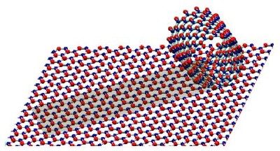
Structural models of a BN monoatomic sheet and a single-shelled BN nanotube. Alternating B and N atoms are shown in blue and red.


Boron nitrides are now being used in a rather ancient technique, the spinning of textiles into yarns.  They've already done this with CNTs as demonstrated in this video here:


Until recently, high-qualtiy BNNTs could be synthesized only up to a micron ( 1 µm) long. Longer nanotubes were riddled with crystalline defects. A team of materials scientists from four institutions
(The paper is found here) spun a ~1 mm thick yarn that looks like cotton:
This yarn is 3 cm long.  "They're big and fluffy, textile-like" said Kevin Jordan, a staff electrical engineer at Jefferson Lab.  "This means you use commercial textile manufacturing and handling techniques to blend them into things like body armor and solar cells and other applications."

How'd they spin this stuff?  By using a laser aimed at a cake of boron inside a chamber filled with nitrogen gas.  This forms a plume of boron gas that shoots upward.  They then insert a cooled metal wire into the gas, causing the gas to condense into liquid droplets.  The droplets combine with nitrogen to self-assemble into BNNTs.  It's a violent reaction that yields the long nanotubes in milliseconds. 

Mass-production of cheap BNNTs may lead to lighter, faster car frames, affordable space vehicles,  and ultralightweight armor; all promised by CNTs, but with the implication that BNNTs are simply easier to make en masse.  What separates CNTs from BNNTs in terms of utility comes down to electrical properties.  The geometry of CNTs drastically changes their conductivity. whereas BNNTs experience very little conductivity alternations with respect to geometry.  In addition, thanks to their chemical inertness, BNNTs promise "pinpoint precision to attack cancer cells by sticking to tumors, absorbing neutrons from a targeted beam, and generating local alpha radiation to kill cancer cells." (See ScienceNOW )

Wednesday, August 11, 2010

LSA experimental setup and conduction.


They used bare silicon wafers as the starting substrate. The wafers were processed through the laser anneal tool prior to inspection. Firstly, one wafer was wafer at six different temperatures at and around the process center line T°C (T-75°, T-50°, T-25°, T, T+25°, and T+50°); this minimized the effects of incoming wafer qualty on the final surface morphology. 
Wafer Schematics

Fig. 2 shows the anneal splits above. Subsequent LSA experiments utilized one wafer with one or two process conditions to verify whether this characterization is reproducibile, and for further understanding of the variations in the annealing process.

They measured the samples via KLA-Tencor’s Surfscan SP2 unpatterned wafer inspection
system. The scans were done under normal (perpendicular) incidence in high-throughput mode–the optimal scan condition for slip line detection and other shallow defects because of their defect scattering characteristics. Also, they obtained surface morphology information from the haze scattering detected on the SP2 by analyzing the so-called SURFimage (don't know what this). The SURFimage haze maps provided local surface information at pixel-level resolution and sub-nm vertical resolution. The resulting data is presented in 192-bit greyscale for clear visualization of surface variation. Each anneal zone had its haze data obtained through a newly developed capability (developed in-house) that enables local data extraction, analysis, and defect binning of local surface scattering signals using user-defined parameters. From this analysis, they correlated the results to LSA process conditions. Lastly, the authors conducted further corroboration by Scanning electron microscope.

Tuesday, June 29, 2010

UV laser scattering on Laser Spike Annealed wafers: an introduction

As devices continue to shrink towards a true nm region, ultra-shallow and low-restivity junctions become vital to suppress short-channel effects and improve device performance. These junctions are created in part from annealation across the wafer; temperature uniformity and the minimization of pattern density effects are crucial within the 45nm node and beyond. A recently introduced method that does this is the Laser Spike Anneal (LSA). This process enables highely localized elevated temperatures for rapid annealing of implant layers without impacting the process thermal budget. The catch: the rapid heating (inherent within the LSA process) induces slip line defects and other surface damage. This is not conducive toward understanding and characterizing the surface morphology of post-anneal wafers. This problem doesn't arise in more traditional methods such as Atomic Force Microscopy (AFM), which does provide accurate and quantitative surface information, but it's too slow for impatient corporate clients.

Scattering of lasers has long been used for monitoring slip lines and other defects on amorphous substrates. Scattering is highly sensitive to changes in substrate morphology and surface roughness. Researchers commonly call the surface roughness "haze". Full-wafer haze information allows characterization and monitoring of surface quality at production-worthy throughput.

In a paper called "A Novel Method of Characterizing Post-laser Anneal Surface Conditions for the 45nm Process Technology Node" by W-Y Teng, J-H Yeh(United Microelectronics Corporation) and P. Chen, S. Radovanovic, D.K. Chen, H. Cheng, and U. Mahajan (KLA-Tencor Corporation), advanced UV laser scattering is applied to characterize the surface. The authors used high-resolution haze to capture whole-wafer surface data at sub-nm resolution. This surface condition presented good correlation with the LSA processing conditions. The results were further confirmed by scanning electron microscope, illustrating the potential of using haze for process development, characterization, and monitoring. The next entry will detail the experimental details.