Showing posts with label Wafer. Show all posts

Sunday, September 19, 2010

CNT Loudspeakers

This seems to be something straight out of science fiction, but they've actually done it. Some smart researchers in China have figured out how to create an entire speaker out of carbon nanotubes. A piece of carbon nanotube thin film could be a practical magnet-free loudspeaker simply by applying an audio current through it. These nanotech loudspeakers (merely 10s of nm thick) can be manipulated into any shape and size while exhibiting flexibility, transparency, and stretchability. They can be mounted onto room walls, ceilings, pillars, windows, flags, and clothes without much area limitations.


In 2002, a group of Chinese researchers developed a technique for creating nanotube yarns up to 30 cm long. They drew the yarns out from super-aligned arrays of CNTs (I guess you can call this nano-knitting). Super-aligned CNT arrays differ from ordinary vertically-aligned CNTs in that their alignment is far superior to that of ordinary CNT arrays. This is important for continuous thin films, or ribbons (composed of parallel pure CNTs); in that they can can be drawn from super-aligned arrays in the solid state. These thin films are transparent and conductive, with aligned CNTs parallel to the drawing direction.

Three years later, the same group of scientists successfully synthesized super-aligned CNT arrays on 4-inch silicon wafers. One such wafer is capable of being transformed into a continuous thin film with dimensions of 10 cm wide by 60 m long (yes, sixty meters).

In 2007, Dr. KaiLi Jiang, the head of the research group and associate professor of physics at Tsingua University in Beijing, had discovered that a piece of a CNT thin film can emit sound by applying an audio frequency current through it, with the interesting of effect of the sound frequency being double the current frequency. This is attributed to the thermoacoustic effect. The alternating current periodically heated the CNT thin films, resulting in temperature oscillation. Said Dr. Jiang: "The temperature oscillation of the thin excites the pressure oscillation in the surrounding air, resulting in sound generation."

Jiang also said that the thermoacoustic effect has been studied for more than 200 years, has led to the invention of thermoacoustic engines and even loudspeaker driven refrigerators.

What remained obscure in the scientific literature is the use of alternating current in thermoacoustic generation. Jiang and his team believed they were the first to discover this effect, but they were beaten by Arnold and Crandall in the late 19th century. A & C used ultra-thin foils made of platinium to feed the current through, which then generated a very weak thermoacoustic effect; too weak for practical use. A & C claim that the sound efficiency is inversely proportional to the heat capacity per unit area (HCPUA) for the material studied. For 700 nm thick platinum foil the HCPUA value is 260 times weaker than for CNTs at the same power input.

The loudspeakers were fabricated by placing the as-drawn CNT thin film on two electrodes, forming a simple loudspeaker. Several thin films were placed together so as to increase the loudspeaker area. The films could be formed into arbitrary shapes or placed on arbitrarily curved surfaces to make loudspeakers with special functions.
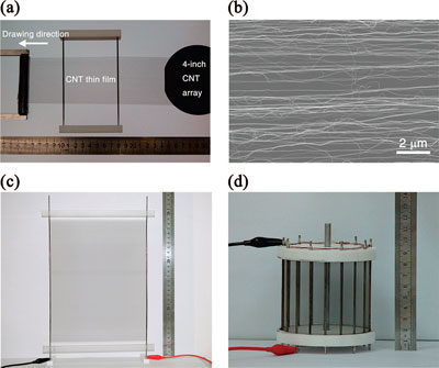
Carbon nanotube thin film loudspeakers. (a) The CNT thin film was pulled out from a super-aligned CNT array grown on a 4 inch silicon wafer and put on two electrodes of a frame to make a loudspeaker. (b) SEM image of the CNT thin film showing that the CNTs are aligned in the drawing direction. (c) A4 paper size CNT thin film loudspeaker. (d) The cylindrical cage shape CNT thin film loudspeaker can emit sounds to all directions, diameter 9 cm, height 8.5 cm. (Reprinted with permission from American Chemical Society). 


The CNT loudspeakers exhibit volumes and frequencies that are quite pleasing to the human ear.   When connected to a simple amplifier, the CNT thin film speaker shares all the functions of a voice-coil loudspeaker, plus the bonuses of no magnet, and no moving parts.  In contrast to conventional loudspeakers, they are stretchable, transparent, and flexible.  CNT loudspeakers also don't vibrate and are quite durable;  they can work even if part of the thin film is torn or damaged.  The possibilities are endless for CNT loudspeaker applications.  E.g., laptop computers where the current audio system is replaced by simply placing a transparent loudspeaker over the screen itself, or for tomorrow's mobile devices such as the Nokia Morph.

The team hopes to develop real commercial products with CNT loudspeakers.  This article is two years old, so progress on this front is currently unknown.  An update will appear here as soon as I hear of it. 

Wednesday, August 11, 2010

LSA experimental setup and conduction.


They used bare silicon wafers as the starting substrate. The wafers were processed through the laser anneal tool prior to inspection. Firstly, one wafer was wafer at six different temperatures at and around the process center line T°C (T-75°, T-50°, T-25°, T, T+25°, and T+50°); this minimized the effects of incoming wafer qualty on the final surface morphology. 
Wafer Schematics

Fig. 2 shows the anneal splits above. Subsequent LSA experiments utilized one wafer with one or two process conditions to verify whether this characterization is reproducibile, and for further understanding of the variations in the annealing process.

They measured the samples via KLA-Tencor’s Surfscan SP2 unpatterned wafer inspection
system. The scans were done under normal (perpendicular) incidence in high-throughput mode–the optimal scan condition for slip line detection and other shallow defects because of their defect scattering characteristics. Also, they obtained surface morphology information from the haze scattering detected on the SP2 by analyzing the so-called SURFimage (don't know what this). The SURFimage haze maps provided local surface information at pixel-level resolution and sub-nm vertical resolution. The resulting data is presented in 192-bit greyscale for clear visualization of surface variation. Each anneal zone had its haze data obtained through a newly developed capability (developed in-house) that enables local data extraction, analysis, and defect binning of local surface scattering signals using user-defined parameters. From this analysis, they correlated the results to LSA process conditions. Lastly, the authors conducted further corroboration by Scanning electron microscope.

Tuesday, June 29, 2010

UV laser scattering on Laser Spike Annealed wafers: an introduction

As devices continue to shrink towards a true nm region, ultra-shallow and low-restivity junctions become vital to suppress short-channel effects and improve device performance. These junctions are created in part from annealation across the wafer; temperature uniformity and the minimization of pattern density effects are crucial within the 45nm node and beyond. A recently introduced method that does this is the Laser Spike Anneal (LSA). This process enables highely localized elevated temperatures for rapid annealing of implant layers without impacting the process thermal budget. The catch: the rapid heating (inherent within the LSA process) induces slip line defects and other surface damage. This is not conducive toward understanding and characterizing the surface morphology of post-anneal wafers. This problem doesn't arise in more traditional methods such as Atomic Force Microscopy (AFM), which does provide accurate and quantitative surface information, but it's too slow for impatient corporate clients.

Scattering of lasers has long been used for monitoring slip lines and other defects on amorphous substrates. Scattering is highly sensitive to changes in substrate morphology and surface roughness. Researchers commonly call the surface roughness "haze". Full-wafer haze information allows characterization and monitoring of surface quality at production-worthy throughput.

In a paper called "A Novel Method of Characterizing Post-laser Anneal Surface Conditions for the 45nm Process Technology Node" by W-Y Teng, J-H Yeh(United Microelectronics Corporation) and P. Chen, S. Radovanovic, D.K. Chen, H. Cheng, and U. Mahajan (KLA-Tencor Corporation), advanced UV laser scattering is applied to characterize the surface. The authors used high-resolution haze to capture whole-wafer surface data at sub-nm resolution. This surface condition presented good correlation with the LSA processing conditions. The results were further confirmed by scanning electron microscope, illustrating the potential of using haze for process development, characterization, and monitoring. The next entry will detail the experimental details.