Wednesday, December 1, 2010

Plasmonics at the bottom: shrinking wavelengths

Plasmonics may be older than you think.  Alchemists and glassmakers spent millennia taking advantage of plasmonic effects when they created stained-glass windows and colorful goblets that incorporated small metallic particles in the glass. By analogy, ignorance of modern biology did not stop Stone-Age humans from genetically engineering wolves and various plants (via selective breeding) to become dogs and farming crops.   Best known example of alchemical plasmonics is the Lycurgus cup, a Roman goblet dating from the 300s A.D.; now held in the British museum.  Thanks to plasmonic excitation of electrons in the metallic particles suspended in the glass, the cup absorbs and scatters blue and green light (relatively short wavelengths in the visible spectrum).  When viewed in reflected light, the plasmonic scattering gives the cup a greenish hue, but if a normal light source (emits white light) is placed inside the goblet, the glass appears red because it transmits only the longer wavelengths (red) and absorbs the shorter ones (green/blue).

Lycurgus Cup: a Roman goblet dating from the 4th century A.D.  It changes color because of the plasmonic excitation of metallic particles within the glass matrix.  When a light source is placed inside the normally green goblet, it looks red.
 Surface plasmon research began with a bang in the 1980s, as chemists studied the phenomenon using Raman spectroscopy: the scattering of laser light off a sample to determine its structure from molecular vibrations.  In 1989, Thomas Ebbesen, then at the NEC Research Institute in Japan, discovered that when he illuminated a thin but opaque gold film imprinted with millions of microscopic holes, the foil somehow transmitted more light than was expected from the number and size of the holes.  This phenomenon, now known as extraordinary optical transmission, was eventually found to be caused by surface plasmons that intensified the transmission of electromagnetic energy.

Then came the discovery of novel "metamaterials": materials in which electron oscillations can result in some weird optical effects.  Their optical effects are so complex (due to plasmons) they require astronomically powerful computers for accurate simulation, but studying them has become less daunting by novel methods for constructing nanoscale structures that allow researchers to build and test ultrasmall plasmonic devices and circuits.

In most circumstances, it would be unwise to use metallic structures to transmit light signals because metals are known for high optical losses (signal weakens after each bounce off the metallic surface until evanescence).  However, when a thin film is combined with an electrical insulator, optical losses decrease due to the electromagnetic (EM) field spreading into the insulating material, where there are no conducting electrons  to oscillate, thus no energy-dissipating collisions.  This property naturally confines plasmons to the metallic surface adjoining the insulator; e.g., in the the top portion of the figure below (PLANAR WAVEGUIDE), the surface plasmons propagate only in the thin plane at the interface.  Note that in this example, the insulator is air. 

With this planar structure acting as a waveguide, shepherding the EM waves along the metal-dielectric boundary, it may be useful in routing signals on a chip.  Most optical signals may attenuate rapidly in metals, but the exception here is a plasmon traveling in a thin-film metal waveguide, whose journey can last for several cm.  The plasmon signal can be made to last longer  if the waveguide employs an asymmetric mode,  meaning the EM energy disperses more intensely in a certain direction than others.  This mode pushes a greater portion of the EM energy away from the guiding metal film and into the surrounding insulator, thus delaying attenuation a little longer.  The EM fields at the top and bottom surfaces of the metal film are known to interact with each other, and this interaction can be manipulated by changing the thickness of the film, which manifests as different frequencies and wavelengths for the plasmons.  In fact, this has already been done in the late '90s by a Danish/Canadian collaboration; they created a planar plasmon waveguide like in the top of the figure, but the EM fields it generated were too large to convey signals through the nanoscale innards of a processor.

Plasmons can propagate through nanoscale wires, but they require more complex waveguide geometries than that of the planar form; plasmons can shrink the wavelength of the optical signal by squeezing it into a narrow space.  This is seen in the middle illustration of the above figure.  This device is called a plasmon slot waveguide; the plasmon wavelength changes with respect to the thickness of the insulator core in the middle.  This is capable of transmitting a signal 10s of microns long (1 micron = 1 µm ≈ diameter of a blood cell).  Now comes the juicy part: a Japanese researcher had managed to squeeze red light (wavelength of 651 nm) into a plasmon slot waveguide that was only 3 nm thick and 55 nm wide.  The wavelength of the surface plasmon propagating through the device was 51 nm, or 8% of the original red light wavelength.  But the frequency remains the same, which means information gets transmitted.  This striking ability to shrink the wavelength opens the floodgates for nanoscale plasmonic structures to perhaps replace purely electronic circuits containing wires and transistors. 

Mass-production of plasmon slot waveguides is another story, but it should be similar to lithography (used to imprint circuit patterns on silicon chips).  This process could mass-produce miniuscule plasmonic devices with arrays of narrow insulating stripes and gaps.  These arrays would guide the waves of positive and negative charges on the metal surface; their behavior is similar to alternating current traveling along an ordinary wire.  However, since the frequency of an optical signal is so much higher than that of an electrical signal (400,000 GHz vs. 60 Hz, respectively),  the plasmonic circuit can carry tons more data.  Additionally, electrons  don't travel from one end of a plasmonic circuit to another; rather, they clump together and spread apart (thus no net directional surface current).  This fact accounts for the device's immunity to resistance and capacitance effects that limit the data-carrying capacity of integrated circuits with electrical interconnects.

Friday, November 5, 2010

Plasmonics at the bottom? Part one.

According to Thomas Friedman, one reason why the world got flat is the mass installation of optical fibers that now span the globe; fibers that guide light signals conveying voluminous streams of voice communications and gigantic amounts of data.  Some researchers believe that such colossal capacity in photonic devices (able to channel and manipulate electromagnetic radiation like light) could someday replace electronic circuits in microprocessors and other computer chips.  Why haven't they already?  Because of the diffraction limit, which constrains the size and performance of photonic devices due to interference between closely-spaced light waves.  The width of an optical fiber carrying closely space light waves must be at least half the light's wavelength inside the material.  Chip-based optical signals usually employ near infared wavelengths of 1.5 µm (micrometers, or millionths of meter–a common unit in cell biology), which far exceeds typical dimensions of base components in most electronic devices being used today–certainly in my computer.

However, scientists have kept busy.  In the 1980s, researhers experimentally confirmed that directing light waves at the interface between a meter and a dielectric (a nonconductive material such as air, glass, or highly pure water) can, if conditions are right, induce a resonant interaction between the waves and the mobile electrons at the metal's surface.  This means that the oscillations of electrons at the surface match those of the electromagnetic field (read: waves) outside the metal.  We now have surface plasmons:  density waves of electrons that propagate along the interface like the ripples that spread across the surface of a pond after a rock splashes into it. 

Recently, scientists discovered that a fine-tuned metal-dielectric interface can generate surface plasmons with the same frequency as the outside electromagnetic (EM) waves, but with a much shorter wavelength.  This effect may enable the plasmons to travel along nanoscale wires called interconnects, carrying information from one section of a microprocessor to another.  I could sense chip designers salivating over these interconnects; they're still making ever smaller and faster transistors, but it's now harder to to build minute electronic circuits that can move data quickly across the chip.

Ten years ago, Professor Atwater and colleagues at Caltech named this emerging discipline "plasmonics", sensing a research pathway may lead to a new class of devices.  One day, plasmonic components might be vital in a diverse set of instruments, using them to improve the resolution of microscopes, LED efficiency, and the sensitivity for chemical and biological detectors.  Plasmonics are even being considered for medical applications; e.g., tiny particles designed for plasmon resonance absorbion to kill cancerous tissues.  Then there's the invisibility cloaks, but that'll be discussed in a future entry, which will be quite soon.

In meantime, here's a nice artist's rendering of a light beam striking a metal surface, thereby generating a plasmon, which is also awkwardly called an electron density wave.  If the light beam is focused on a surface with a circular grove, as shown here, it produces concentric waves, organizing the electrons into high- and low-density rings.

Tuesday, October 12, 2010

Boron Nitride nanotubes

I wrote about CNTs in my last post; figured it was inevitable since they get so much press.  I've been binging on Skeptics Guide to the Universe recently.  They're a weekly podcast that covers pseudoscience and various shenanigans in the world of nonsense.  Each podcast concludes with a segment known as "Science, or, Fiction", in which the SGU members guess which of the three science news stories is fiction (I should use this when I'm the tabletopics master in a Toastmasters meeting).  One podcast from earlier this year had a S or F story about boron nitride nanotubes, which I've never heard before.  I correctly guessed this is science, since I haven't yet heard a materials science article of their selection that turned out to be fiction. 


So, what the heck are boron nitride nanotubes? Well, to start, boron nitride (BN) is a binary chemical compound consisting of equal proportions of boron and nitrogen. It's the white material used in clown makeup and face powder.   It's isoelectronic (shares the number of electrons) with carbon, and can morph into similar physical structures: graphene-like, and diamond-like.  The latter  is the only material nearly as hard as diamond.  It remains a solid at temperatures up to 1000ºC for air, and up to 1800ºC in an inert gas atmosphere.  That's twice as high for carbon nanotubes. 

If you look for carbon on the periodic table, you may see boron is on its left, and nitrogen is on its right.  Carbon has four electrons in its valence shell, which means another four is needed to satisfy the octet rule.  Thus, boron has three valence electrons, and nitrogen has five.  Combining these two atoms satisfies the octet rule.  By extension, BN can form a graphene (1 atomic layer of graphite) lattice.  But what makes BN different from its carbon analogues is its wide band gap of approx. 5.5 eV, making a wide-gap semiconductor (effectively an insulator). 

The high bandgap for BN nanotubes (BNNT) is a factor behind their high thermal and chemical stability.  They also have excellent mechanical properties and high thermal conductivity, much like carbon nanotubes. 

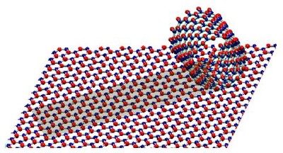
Structural models of a BN monoatomic sheet and a single-shelled BN nanotube. Alternating B and N atoms are shown in blue and red.


Boron nitrides are now being used in a rather ancient technique, the spinning of textiles into yarns.  They've already done this with CNTs as demonstrated in this video here:


Until recently, high-qualtiy BNNTs could be synthesized only up to a micron ( 1 µm) long. Longer nanotubes were riddled with crystalline defects. A team of materials scientists from four institutions
(The paper is found here) spun a ~1 mm thick yarn that looks like cotton:
This yarn is 3 cm long.  "They're big and fluffy, textile-like" said Kevin Jordan, a staff electrical engineer at Jefferson Lab.  "This means you use commercial textile manufacturing and handling techniques to blend them into things like body armor and solar cells and other applications."

How'd they spin this stuff?  By using a laser aimed at a cake of boron inside a chamber filled with nitrogen gas.  This forms a plume of boron gas that shoots upward.  They then insert a cooled metal wire into the gas, causing the gas to condense into liquid droplets.  The droplets combine with nitrogen to self-assemble into BNNTs.  It's a violent reaction that yields the long nanotubes in milliseconds. 

Mass-production of cheap BNNTs may lead to lighter, faster car frames, affordable space vehicles,  and ultralightweight armor; all promised by CNTs, but with the implication that BNNTs are simply easier to make en masse.  What separates CNTs from BNNTs in terms of utility comes down to electrical properties.  The geometry of CNTs drastically changes their conductivity. whereas BNNTs experience very little conductivity alternations with respect to geometry.  In addition, thanks to their chemical inertness, BNNTs promise "pinpoint precision to attack cancer cells by sticking to tumors, absorbing neutrons from a targeted beam, and generating local alpha radiation to kill cancer cells." (See ScienceNOW )

Sunday, September 19, 2010

CNT Loudspeakers

This seems to be something straight out of science fiction, but they've actually done it. Some smart researchers in China have figured out how to create an entire speaker out of carbon nanotubes. A piece of carbon nanotube thin film could be a practical magnet-free loudspeaker simply by applying an audio current through it. These nanotech loudspeakers (merely 10s of nm thick) can be manipulated into any shape and size while exhibiting flexibility, transparency, and stretchability. They can be mounted onto room walls, ceilings, pillars, windows, flags, and clothes without much area limitations.


In 2002, a group of Chinese researchers developed a technique for creating nanotube yarns up to 30 cm long. They drew the yarns out from super-aligned arrays of CNTs (I guess you can call this nano-knitting). Super-aligned CNT arrays differ from ordinary vertically-aligned CNTs in that their alignment is far superior to that of ordinary CNT arrays. This is important for continuous thin films, or ribbons (composed of parallel pure CNTs); in that they can can be drawn from super-aligned arrays in the solid state. These thin films are transparent and conductive, with aligned CNTs parallel to the drawing direction.

Three years later, the same group of scientists successfully synthesized super-aligned CNT arrays on 4-inch silicon wafers. One such wafer is capable of being transformed into a continuous thin film with dimensions of 10 cm wide by 60 m long (yes, sixty meters).

In 2007, Dr. KaiLi Jiang, the head of the research group and associate professor of physics at Tsingua University in Beijing, had discovered that a piece of a CNT thin film can emit sound by applying an audio frequency current through it, with the interesting of effect of the sound frequency being double the current frequency. This is attributed to the thermoacoustic effect. The alternating current periodically heated the CNT thin films, resulting in temperature oscillation. Said Dr. Jiang: "The temperature oscillation of the thin excites the pressure oscillation in the surrounding air, resulting in sound generation."

Jiang also said that the thermoacoustic effect has been studied for more than 200 years, has led to the invention of thermoacoustic engines and even loudspeaker driven refrigerators.

What remained obscure in the scientific literature is the use of alternating current in thermoacoustic generation. Jiang and his team believed they were the first to discover this effect, but they were beaten by Arnold and Crandall in the late 19th century. A & C used ultra-thin foils made of platinium to feed the current through, which then generated a very weak thermoacoustic effect; too weak for practical use. A & C claim that the sound efficiency is inversely proportional to the heat capacity per unit area (HCPUA) for the material studied. For 700 nm thick platinum foil the HCPUA value is 260 times weaker than for CNTs at the same power input.

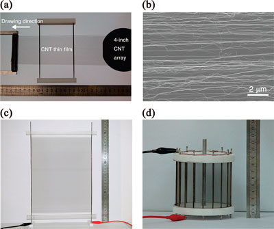
The loudspeakers were fabricated by placing the as-drawn CNT thin film on two electrodes, forming a simple loudspeaker. Several thin films were placed together so as to increase the loudspeaker area. The films could be formed into arbitrary shapes or placed on arbitrarily curved surfaces to make loudspeakers with special functions.

Carbon nanotube thin film loudspeakers. (a) The CNT thin film was pulled out from a super-aligned CNT array grown on a 4 inch silicon wafer and put on two electrodes of a frame to make a loudspeaker. (b) SEM image of the CNT thin film showing that the CNTs are aligned in the drawing direction. (c) A4 paper size CNT thin film loudspeaker. (d) The cylindrical cage shape CNT thin film loudspeaker can emit sounds to all directions, diameter 9 cm, height 8.5 cm. (Reprinted with permission from American Chemical Society). 


The CNT loudspeakers exhibit volumes and frequencies that are quite pleasing to the human ear.   When connected to a simple amplifier, the CNT thin film speaker shares all the functions of a voice-coil loudspeaker, plus the bonuses of no magnet, and no moving parts.  In contrast to conventional loudspeakers, they are stretchable, transparent, and flexible.  CNT loudspeakers also don't vibrate and are quite durable;  they can work even if part of the thin film is torn or damaged.  The possibilities are endless for CNT loudspeaker applications.  E.g., laptop computers where the current audio system is replaced by simply placing a transparent loudspeaker over the screen itself, or for tomorrow's mobile devices such as the Nokia Morph.

The team hopes to develop real commercial products with CNT loudspeakers.  This article is two years old, so progress on this front is currently unknown.  An update will appear here as soon as I hear of it. 

Sunday, September 12, 2010

Results and Discussion

Figure 3 shows a Light Point Defect (LPD) map for the first wafer used in the study. The wafer has typical edge defects, but the LPD map doesn't show noticeable differences among the various anneal process conditions (zones). This implies that any modification to the wafer surface that might have occurred during the laser anneal is below the detection threshold of the defect channel.

However, the SURFimage wafer map (see Fig. 4) shows distinct visual  differences among the different process zones on the wafer.  The average haze from each process zone was plotted against the LSA temperature.

The figure above shows wide channel haze versus process temperature.  It also shows strong correlation between the scattering signal and the anneal temperature. 

Previous studies have shown a good correlation between the so-called power spectral density (PSD) and surface roughness as measured by laser scattering.  Based on these studies and on this work, the haze results indicate that the wafer surface is modified and roughened by the LSA process. Therefore, the surface roughening increases with LSA temperature.

The authors then reviewed the different zones by SEM to better understand the surface features on the annealed wafer.  The results in Fig. 6 show increased surface topography and modification for the zones annealed at higher temperatures.

 More annealed wafers (Fig. 7) show similar correlation between LSA temperature and SP2 (?) haze, which shows that this technique is repeatable. 

The figure above also shows the raster pattern on the wafer.  This technique is also effective at capturing within wafer variations in the surface morphology.  A wafer that was annealed at T-75ºC was scanned in high-sensitivity mode on the SURFscan SP2.  The SURFimage map (Fig. 8) is effectively able to detect annealing variations within the wafer via changes in the local haze.


The second map shows the wafer binned into low, medium, and high haze regions for ease of view.  These results show the ability of SURFimage to provide full-wafer surface information at industrial scale throughputs.

Following this study is planned AFM analysis of the different LSA zones in order to obtain a direct quantitative correlation between the measured surface roughness and haze.  Also, the amorphous wafer defectiveness and surface morphology will be also correlated to inline product wafer inspection results.  At 45 nm, surface morphology requirements become increasingly strigent.  The results here can establish SPC limits for production monitoring of the LSA process. 

Conclusion

As ICs shrink to nearly molecular scales, understanding and characterizing the impact of process variations on wafer surface conditions and identifying potential surface damage becomes critical.  UV laser scattering technology enables full-wafer surface monitoring with sub-nm vertical resolution and high throughput.   This technique can be quite sensitive to small variations in LSA process temperatures that wouldn't be detected by standard defect-monitoring methods; we got ourselves a powerful new tool for process development and monitoring in a fab production environment. 

Wednesday, August 11, 2010

LSA experimental setup and conduction.


They used bare silicon wafers as the starting substrate. The wafers were processed through the laser anneal tool prior to inspection. Firstly, one wafer was wafer at six different temperatures at and around the process center line T°C (T-75°, T-50°, T-25°, T, T+25°, and T+50°); this minimized the effects of incoming wafer qualty on the final surface morphology. 
Wafer Schematics

Fig. 2 shows the anneal splits above. Subsequent LSA experiments utilized one wafer with one or two process conditions to verify whether this characterization is reproducibile, and for further understanding of the variations in the annealing process.

They measured the samples via KLA-Tencor’s Surfscan SP2 unpatterned wafer inspection
system. The scans were done under normal (perpendicular) incidence in high-throughput mode–the optimal scan condition for slip line detection and other shallow defects because of their defect scattering characteristics. Also, they obtained surface morphology information from the haze scattering detected on the SP2 by analyzing the so-called SURFimage (don't know what this). The SURFimage haze maps provided local surface information at pixel-level resolution and sub-nm vertical resolution. The resulting data is presented in 192-bit greyscale for clear visualization of surface variation. Each anneal zone had its haze data obtained through a newly developed capability (developed in-house) that enables local data extraction, analysis, and defect binning of local surface scattering signals using user-defined parameters. From this analysis, they correlated the results to LSA process conditions. Lastly, the authors conducted further corroboration by Scanning electron microscope.

Tuesday, June 29, 2010

UV laser scattering on Laser Spike Annealed wafers: an introduction

As devices continue to shrink towards a true nm region, ultra-shallow and low-restivity junctions become vital to suppress short-channel effects and improve device performance. These junctions are created in part from annealation across the wafer; temperature uniformity and the minimization of pattern density effects are crucial within the 45nm node and beyond. A recently introduced method that does this is the Laser Spike Anneal (LSA). This process enables highely localized elevated temperatures for rapid annealing of implant layers without impacting the process thermal budget. The catch: the rapid heating (inherent within the LSA process) induces slip line defects and other surface damage. This is not conducive toward understanding and characterizing the surface morphology of post-anneal wafers. This problem doesn't arise in more traditional methods such as Atomic Force Microscopy (AFM), which does provide accurate and quantitative surface information, but it's too slow for impatient corporate clients.

Scattering of lasers has long been used for monitoring slip lines and other defects on amorphous substrates. Scattering is highly sensitive to changes in substrate morphology and surface roughness. Researchers commonly call the surface roughness "haze". Full-wafer haze information allows characterization and monitoring of surface quality at production-worthy throughput.

In a paper called "A Novel Method of Characterizing Post-laser Anneal Surface Conditions for the 45nm Process Technology Node" by W-Y Teng, J-H Yeh(United Microelectronics Corporation) and P. Chen, S. Radovanovic, D.K. Chen, H. Cheng, and U. Mahajan (KLA-Tencor Corporation), advanced UV laser scattering is applied to characterize the surface. The authors used high-resolution haze to capture whole-wafer surface data at sub-nm resolution. This surface condition presented good correlation with the LSA processing conditions. The results were further confirmed by scanning electron microscope, illustrating the potential of using haze for process development, characterization, and monitoring. The next entry will detail the experimental details.