Sunday, March 11, 2012

Femtosecond laser ablation

My research will be on organic coatings.  This is the first such post.

As commonly as coatings are used, their weathering-induce degradation is complex and thus remains poorly understood, as coatings can fail in a variety of ways (I think that's what they mean by 'failure modes').  Barrier properties of the coating system can be compromised, along with its mechanical properties.  Proper evaluation of durability and longevity of modern composite coating systems requires characterization of weather/aging phenomena as a function of their spatial distributions.  In the case(s) of homogenous organic coatings, or for coatings with low pigment-to-volume concentrations (PVC), this is typically performed by spectroscopic analysis to cross-sectional samples or by a form of confocal spectroscopy.  Those techniques are fine and dandy if the coating cross-sections are transparent.  If opaque, better get creative, which a team of researchers from SUNY Stony Brook did so.

Background
UV-induced aging of polymeric coatings significantly changes the chemical and morphological structure within the organic matrix of the coating.  Many coatings are based on aromatic ring structures, and are prone to UV absorption and yellowing.  Even aliphatic binders are prone to UV-induced weathering, although to a lesser degree.  Either way, our understanding of these physiochemical changes remain murky; we can't predict if a polymer chain within the coating will cross-link or undergo scission.  
Degradation of composite coatings are even harder to understand; these are coatings that contain a disproportionate amount of inorganic components.  The mechanism depends on both the base chemistry of the organic binder, and on the characteristics of the inorganic additives contained within the coating.  Below is a schematic of such a coating system.  

Most of my research may focus on coatings for military vehicles, so this should be a good model to use in this article.
The closer you get to the surface coating, the more degradation–in other words, weathering/aging also depends on depth.  
Thus, it's best to design a method that yields spectral data and data of the spatial distribution throughout the coating system.  We may a few such depth-profiling techniques already: confocal focusing of an energy beam probe (Confocal Raman Spectroscopy), Secondary Ion Mass Spectroscopy (SIMS), and transmission-mode Fourier Transform Infrared Spectroscopy (transmission-mode FTIR), and UV-Visble spectroscopy.  CRS requires transparent samples, thus out of the question; SIMS won't work for dielectric coatings (practically all organic coatings).  
Transmission-mode FTIR and UV-Visible spectroscopy work well, but they require intact cross-sections with dimensions too small for practical preparation.  A simpler preparation involves microtoming at very small angles to the surface of the coating–effectively extending the depth of the sample to a degree that enables usage of attenuated total reflectance FTIR, but that opens up another can of worms: interlayer mixing due to the microtome blade.  Materials that are too hard and incohesive to microtome successfully are equally vexed when a spectroscopic profile is demanded.  To meet this demand, Keenes et al devised a novel use of a femtosecond (10-15 sec) pulsed laser as an enabler for depth-profiling coatings of this type.
This isn't the first time they used lasers for ablation; previous time scales include nanoseconds (10-9 sec) and picoseconds (10-12 sec).  Laser ablation isn't entirely understood, but it's believed to be the result of a coulombic explosion, in which near-instantaneous ionization of atoms via bright laser beam excites electrons to the point of escaping from their host atoms.  The atoms have become so ionized as to be repulsed by the neighboring positive charges on the irradiated material–repulsions with pressures 10 million times that of standard atmospheric pressure.  This results in a direct solid-to-vapor transition characterized by a violent release of ions from the surface.
Now, people have used ultra-fast laser ablation before, but in the context of mass spectroscopy.  Keenes et al extend this technique to infrared spectroscopy, which is the kind of data that explains the depth profile of the coating.  They hope no post-ablation thermal disruptions will alter the coating composition.
Why do they care about what a coating looks like underneath its surface?  Well, when your client is the U.S. military, you have many reason$ to care.  The scientific reasons will be explained in the next paragraph.  The coatings in question are commonly used on fixed wing/rotary aircraft and naval vessels.  Femtosecond laser ablation is supposed to reveal the underlying layers of the coating to be analyzed ATR-mode FTIR to investigate the depth to which photooxidation of the organic binder has occurred.  A binder is a resin used to keep particles together and supply mechanical strength or to ensure uniform consistency, solidification, or adhesion to a surface coating.
The military coating studied here is a chemical agent resistant coating (CARC) comprising of low-gloss automotive-grade aliphatic polyurethane highly loaded with a pigmentation/filler package.  It seems that this coating in question in part stems from a 1970s patent on tri-functional isocyanate cross linking agents (a bit too technical to delve into for a blog entry).  The main pigment in this coating is a nanoscale spherical titanium dioxide that bestows a light gray color to the coating for optical camouflage.  Diatomaceous earth is added to the coating to lower the gloss (high gloss is bad for camo). SEM micrographs of the coating in question is provided below.
 SEM micrograph (top) of coating cross-section. High volumetric proportion of pigmentation/inorganic fillers is evident from the three EDS elemental maps of Ti (pigment), Si (pigment C flattening agent) and Ca (flattening agent). 
In addition to optical/infrared camouflage, the military uses coatings for protection of metal substrate from corrosion/weathering and resistance to perforation by chemical decontamination agents.  Uncle Sam also demands that its colors don't wash or fade out and it can maintain its mechanical integrity according to appropriate specifications.  This coating has seen extensive action in weathering studies by Keene et al, so it serves as a useful model for this ablation technique to investigate.  Experimental Results and discussion will be detailed in the next entry.  

It's nice to be back!  

Monday, March 14, 2011

Nanocars!

Researchers at the Rice University embarked on a 'fantastic voyage' toward miniaturizing the beloved car to a scale that would be considered science fiction 20 years ago.  In 1998, principal investigator James Tour, professor of organic chemistry at Rice, began this journey.  It took his group eight years to synthesize a functional nanocar.  The goal was to create a nanomachine capable of converting energy-inputs (such as heat or electric fields) into controlled motion on a surface and transport cargo from one place to another on a surface.  Future nanomachine development depends on this because the bottom-up constructions may occur on the surface of semiconductors, metals, or biological and artificial membranes.  Thus, acquring better data on the chemistry and physics on nano-transporters on surfaces is critical; the creation of nanocars is an initial, but significant, step in this scientific frontier.  Nanocars allow us find out basic rules for their design and operation. 

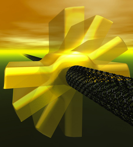
The basic design of a nanocar is much like a real car: it has a  chassis and four axles, except that it's made out of organic groups with pivoting suspension and the axles freely rotate.  The wheels are buckyballs, The entire car measures just 3-4 nm across, just wider than a strand of DNA. 

Though laborious measurements on the STM, the researchers proved that the cars rolled on the surface rather than slide across as previously predicted.  Of course, they had to raise the temperature of the gold surface to 200 ºC, but they were still able to determine that it was easier to move the car forward or backward rather than sideways.   


Monday, February 21, 2011

Molecular Machinery: A Brief Overview

Functional molecular devices have been designed and fabricated for several years now:
Gold nanorotor
Nanoswitch

Such nano versions of macroscopic machines are in part inspired by the visionary physicist Richard Feynman 50 years ago.  Also, fabrication and synthesis technologies has advanced enough to initialize and perpetuate the quest to miniaturize machinery in the current science and engineering disciplines. 

One of the most advanced current fabrication meths, the "top-down approach to miniturization in the semiconductor industry, is approaching the limits in scaling. For example, the band structure of silicon disappears when silicon layers are just a few atoms thick.  What about photolithography?  Well, its operational wavelengths are too limited for making nanomachines with moving parts.  

Recently, organic chemists in Rice University realized they can synthesize 3 × 4 nm nanocars in 100 mL laboratory reaction flasks–30 mg worth (that translates into 3 × 10¹⁸ nanocars–far exceeding the number of automobiles made in the history of the world.).  30 nanocars, side by side, can span the 90 nm width of a small in line in the most advanced logic chip being made today.  Tiny objects with many moving parts like nanocars have to be made differently, from the "bottom-up".  This follows more naturally in line with Darwinian evolution at the biochemical level, although we're nowhere near the sophistication of Nature's handiwork.  Consequently, molecular scientists have turned their attention to much simpler systems, where the machinery may be easier to construct and understand, perhaps serving as a base for eventual progression toward sophisticated and useful nanomachines.  

Most of the molecular machines shown above were designed and synthesized to operate in the liquid phase because of the abundant tools available to analyze products in solution.  However, useful nanomachines with mechanical functions require eventual integration into devices that interface surrounding systems (likely to operate in the solid phase).  For example, the biological nanomachine ATPase is anchored in a biological membrane in order to connect with its surroundings.  Overcoming this interface problem ranks among the most intractable of problems in nanomachine design.  

Nevertheless, there are several viable designs that (1) work in a crystalline solid, or (2) be mounted on and operated on surface, or (3) move around and operate on a surface.  
 
Machines operating in crystalline solid state
UCLA researchers have made considerable progress in the formulation, design, and preparation of crystalline molecular machines.  Examples of their work include molecular compasses and gyroscopes.  

The center component of the molecule above (red) has a magnetic moment that responds via rotation to external magnetic fields.  The plot qualitatively indicates the energy required for the rotation to occur. 

 Conventional crystalline materials have their molecular components tightly bonded and restricts their motion, which contrasts to another class of materials known as amphidynamic crystals.  These exotic crystals possess rigid lattices connected to moving parts (See pic below).   
Example of an amphidynamic crystal

Successful utilization of such crystals will lead to photonics materials whose components  stem from the bulk (not from solution or thin films), which increases the density, which leads to greater advances.  


Machines mounted and operating on a surface

Molecular machines heavily depend on positioning to be to pump, push, lift materials, or other useful work.  Examples of such machines already produced in the lab are: (see captions of following pictures)
cyclodextrin necklaces. 
J. Am. Chem. Soc. 2000, 122, 5411-5412
Molecular Shuttles,     http://www.ch.nagasaki-u.ac.jp/mol/research_e.html
Light powered molecular motor.  The absorption of sunlight by one of the two stoppers, a light-harvesting one, causes the transfer of one electron to station A, which is deactivated as far as wanting the ring to encircle it. As a consequence, the ring moves to its second port of call, station B. Station A is subsequently reactivated by the return of the transferred electron to the light-harvesting stopper, and the ring moves back to this station. Copyright © UCLA
Machines moving and operating on a surface
As if mounting nanomachines on a surface weren't hard enough, people are also trying to make them move and do stuff.  That may call for zealous usage of scanning probes such as the scanning tunneling microscope (STM).  In fact, the STM has been used to push these molecules on a surface laterally, with atomic scale precision.  Perhaps the most famous molecule used for this purpose is the molecular wheelbarrow:


(a) macroscopic wheelbarrow.  Its colors correspond to the chemical structure in (b).  (c) shows the molecule in the gas phase. 
Mechanical interactions between molecule and surface determines the molecule's motion on a variety of surfaces.  For macroscopic objects, the theory and basic rules for the design of machinery is well-known and justly exploited.  Skiing works for snow, but not for asphalt.  On water, wheels only float on their own if they're made of rubber; recommended solution, get a sailboat.  These situations don't require much brainpower to imagine, but rigorous mathematical and physical theories are necessary to explain them.  But on the atomic level, the rules are different, and therefore the normal human intuitions for working machinery do not apply.  Movement on surfaces might not follow Newtonian physics, but rather quantum mechanics.  Quantum calculations are notoriously difficult and computationally costly to obtain exact answers with the currently available tools.  For now, the development of molecular machinery depends mostly on dogged trial-and-error.  

Friday, February 18, 2011

DNA Robospider

The nanites are here, and they're made of DNA.  Well, not really, but researchers at 4 institutions across the country have created and programmed DNA spider-bots that walk independently across a a nano-scale track.  A baby step (spider step?), but also a milestone, in the nascent fields of molecular computing and and robotics.  Eric Drexler had long envisioned molecular robots in his seminal book Engines of Creation, now manifesting into reality. 
Normally, a robot would have a set of instructions to follow specific tasks repeatedly, from vacuuming carpets to welding cars, but programming biomolecules?  Not a simple task, and requires researchers from many disciplines (CS, chemistry, engineering, biology) to collaborate, which did occur.  The result are DNA walkers with 'legs' that allow them to briefly walk autonomously on a fabricated 2D landscape.  They can begin and continue walking, turn, then stop.  Rinse and repeat.  The walkers are only ~ 4 nm in diameter, and walk very slowly, covering 100 nm in 30 minutes to an hour by only 100 steps.   Compare that to previous walkers took that long to walk only 3 nm.
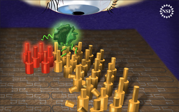
Researchers have created and observed a molecular robot capable of many steps, and of making decisions where to step and how long to stay. As the robot walks on the substrate, it changes each piece by cleaving off a part. If it touches a spot that has been cleaved already, it does not linger as long. The end of the track glows red and captures the robot, letting the researchers know when it has completed its walk. The robot glows green, allowing for the researchers to see it better. Credit: Zina Deretsky, National Science Foundation


This shows high promise for the emerging nanomedicine field, which promises localized cancer treatment.  Imagine a time when we can look back and consider chemotherapy to be barbaric and inhumane.  Nanomedicine could be our ticket to that future. 

Wednesday, December 8, 2010

Plasmonics at the bottom: Nanoshells and Invisibility Cloaks

Plasmonics may have roles to play aside from computing.  Researchers Naomi Halas and Peter Nordlander at Rice University have developed structures called nanoshells that consist of a thin layer of gold coating (usually 10 nm thick) around the entire surface of a silica particle about (100 nm in diameter).  Placing this coated particle in an electromagnetic (EM) field generates electron oscillations in the gold shell; this is due to the coupling interaction between the fields on the shell's inner and outer surfaces.  Varying the silica particle size and the gold layer thickness changes the wavelength at which the particle resonantly absorbs energy.  In short, nanoshells can be designed to selectively absorb wavelengths from the blue end of the visible spectrum (approx. 300 nm), and down to the near infrared (about 10 microns).

Surprisingly enough, nanoshells are now being considered for cancer treatment.  In 2004, Halas, working with Rice colleague Jennifer West, injected plasmonic nanoshells into the bloodstream of mice with malignant tumors and found that the particles were nontoxic.  Moreover, the nanoshells tended to embed themselves in the rodents' cancerous tissues rather than healthy ones due to higher blood circulation in the fast-growing tumors.


Additionally, human and animal tissues are transparent to radiation at certain infared wavelengths.  When near-infrared laser light is aimed at the tumors through the mice's skin, the resonant absorption of energy in the embedded nanoshells raised the temperature of the cancerous tissues from 37 ºC to 45 ºC.

This photothermal heating killed the cancer cells while leaving the surrounding healthy issue intact.  In the mice treated with nanoshells, the tumors virtually disappeared within 10 days; in the control groups, the tumors grew unabated.  As of 2009, practitioners are seeking FDA approval for clinical trials of nanoshell therapy in patients with head and neck cancer.

Plasmonics may also revolutionize the lighting industry by making LEDs bright enough to compete with incandescent bulbs.  In the early '80s, researchers found that the plasmonic enhancement of the electric field at the metal-insulator boundary could make certain dyes more luminescent if placed near the metal's surface.  This kind of plasmonic enhancement can also raise the radiation rate of quantum dots and quantum wells (tiny semiconductor structures that absorb and emit light), which improves the efficiency and brightness of solid-state LEDs.  A recent collaboration between Caltech and Nichia Corporation in Japan demonstrated that coating the surface of a gallium nitride LED with dense arrays of plasmonic nanoparticles (made of gold, silver, or aluminum) could intensify the emitted light 14-fold. 

Additionally, plasmonic nanoparticles may one day lead to LEDs made of silicon.  Silicon-based LEDs would be much cheaper than conventional LEDs composed of gallium nitride or gallium arsenide, but such devices currently emit too little light.  Research has shown that coupling silver or gold plasmonic nanostructures to silicon-dot arrays could boost their photon intensity by 10 times.  Moreover, the frequency of the enhanced emissions can be tuned by adjusting the geometries of the nanoparticles.  Simulations have indicated that careful tuning of the plasmonic resonance frequency combined with precise control of the separation between the metallic particles and the semiconductor materials may allow emission rates to rise more than 100-fold, allowing silicon LEDs to shine just as brightly as traditional devices.

Then there's the plasmonic analogue to a laser.  Mark Stockman of Georgia State University and David Bergman of Tel Aviv University theorized a new device called a SPASER (surface plasmon amplification of stimulated emission of radiation).  They have suggested fabrication methods via semiconductor quantum dots and metal particles.  The radiative energy from the quantum dots would be transformed into plasmons, which would then be amplified in a plasmonic resonator.  The plasmons generated by a SPASER  would be much more tightly localized than a conventional laser beam; this would allow the device to operate at very low power and selectively excite very small objects.  The result: SPASERs may further sensitize spectroscopy to more phenomena and to more sensitive hazardous material-detectors for minute amounts of chemicals or viruses.

Speaking of excitement, plasmonics are a potential candidate for the proverbial invisibility cloak of Hollywood films.  What is taught again and again in freshman physics is the refractive index, which is the ratio of the speed of light in a vacuum to the speed of light in the material.  If the refractive index is made equal to that of air, the object is rendered nearly invisible.  For plasmonic materials, this could be done with two things:
1) Use radiation that is close to the resonant frequency of the structure; it would neither bend nor reflect light.  The light is absorbed, never to bounce back to the observer's eye.
2) Laminate the structure with a material that produces optical gain (amplifying the transmitted signal just as the resonator in a SPASER would); the resulting higher intensity would offset the absorption losses.  The structure is thus rendered invisible, at least to radiation in a selected range of frequencies.

In theory, plasmonic materials could render objects invisible.  In one proposal, the cloaking device would be a thick shell constructed of metamaterials, which exhibit unusual optical properties.  This shell could bend radiation around its central cavity, where a spaceship could be hidden.  A space telescope pointed at the shell would see only the galaxy behind it. 
Now, it's one thing to render an object invisible for a set frequency, but it's quite another to hide it for the entire visible spectrum.  Some physicists say it is possible.  John B. Pendry of Imperial College London and colleagues showed that a shell of metamaterials might, in theory, reroute the electromagnetic waves traveling through it, diverting them around a spherical shell, as seen in the figure above.

Invisibility cloaks may never see the light of day (ha!), but such ideas highlight the wealth of optical properties that inspire scientists working in plasmonics.  By investigating the sophisticated coupling between electrons unbounded to atoms, and electromagnetic waves, researchers have identified new possibilities for transmitting data in our microchips, illuminating our homes, and fighting cancer.  Indeed, there's still a lot of 'room' to explore in plasmonics.

Wednesday, December 1, 2010

Plasmonics at the bottom: shrinking wavelengths

Plasmonics may be older than you think.  Alchemists and glassmakers spent millennia taking advantage of plasmonic effects when they created stained-glass windows and colorful goblets that incorporated small metallic particles in the glass. By analogy, ignorance of modern biology did not stop Stone-Age humans from genetically engineering wolves and various plants (via selective breeding) to become dogs and farming crops.   Best known example of alchemical plasmonics is the Lycurgus cup, a Roman goblet dating from the 300s A.D.; now held in the British museum.  Thanks to plasmonic excitation of electrons in the metallic particles suspended in the glass, the cup absorbs and scatters blue and green light (relatively short wavelengths in the visible spectrum).  When viewed in reflected light, the plasmonic scattering gives the cup a greenish hue, but if a normal light source (emits white light) is placed inside the goblet, the glass appears red because it transmits only the longer wavelengths (red) and absorbs the shorter ones (green/blue).

Lycurgus Cup: a Roman goblet dating from the 4th century A.D.  It changes color because of the plasmonic excitation of metallic particles within the glass matrix.  When a light source is placed inside the normally green goblet, it looks red.
 Surface plasmon research began with a bang in the 1980s, as chemists studied the phenomenon using Raman spectroscopy: the scattering of laser light off a sample to determine its structure from molecular vibrations.  In 1989, Thomas Ebbesen, then at the NEC Research Institute in Japan, discovered that when he illuminated a thin but opaque gold film imprinted with millions of microscopic holes, the foil somehow transmitted more light than was expected from the number and size of the holes.  This phenomenon, now known as extraordinary optical transmission, was eventually found to be caused by surface plasmons that intensified the transmission of electromagnetic energy.

Then came the discovery of novel "metamaterials": materials in which electron oscillations can result in some weird optical effects.  Their optical effects are so complex (due to plasmons) they require astronomically powerful computers for accurate simulation, but studying them has become less daunting by novel methods for constructing nanoscale structures that allow researchers to build and test ultrasmall plasmonic devices and circuits.

In most circumstances, it would be unwise to use metallic structures to transmit light signals because metals are known for high optical losses (signal weakens after each bounce off the metallic surface until evanescence).  However, when a thin film is combined with an electrical insulator, optical losses decrease due to the electromagnetic (EM) field spreading into the insulating material, where there are no conducting electrons  to oscillate, thus no energy-dissipating collisions.  This property naturally confines plasmons to the metallic surface adjoining the insulator; e.g., in the the top portion of the figure below (PLANAR WAVEGUIDE), the surface plasmons propagate only in the thin plane at the interface.  Note that in this example, the insulator is air. 

With this planar structure acting as a waveguide, shepherding the EM waves along the metal-dielectric boundary, it may be useful in routing signals on a chip.  Most optical signals may attenuate rapidly in metals, but the exception here is a plasmon traveling in a thin-film metal waveguide, whose journey can last for several cm.  The plasmon signal can be made to last longer  if the waveguide employs an asymmetric mode,  meaning the EM energy disperses more intensely in a certain direction than others.  This mode pushes a greater portion of the EM energy away from the guiding metal film and into the surrounding insulator, thus delaying attenuation a little longer.  The EM fields at the top and bottom surfaces of the metal film are known to interact with each other, and this interaction can be manipulated by changing the thickness of the film, which manifests as different frequencies and wavelengths for the plasmons.  In fact, this has already been done in the late '90s by a Danish/Canadian collaboration; they created a planar plasmon waveguide like in the top of the figure, but the EM fields it generated were too large to convey signals through the nanoscale innards of a processor.

Plasmons can propagate through nanoscale wires, but they require more complex waveguide geometries than that of the planar form; plasmons can shrink the wavelength of the optical signal by squeezing it into a narrow space.  This is seen in the middle illustration of the above figure.  This device is called a plasmon slot waveguide; the plasmon wavelength changes with respect to the thickness of the insulator core in the middle.  This is capable of transmitting a signal 10s of microns long (1 micron = 1 µm ≈ diameter of a blood cell).  Now comes the juicy part: a Japanese researcher had managed to squeeze red light (wavelength of 651 nm) into a plasmon slot waveguide that was only 3 nm thick and 55 nm wide.  The wavelength of the surface plasmon propagating through the device was 51 nm, or 8% of the original red light wavelength.  But the frequency remains the same, which means information gets transmitted.  This striking ability to shrink the wavelength opens the floodgates for nanoscale plasmonic structures to perhaps replace purely electronic circuits containing wires and transistors. 

Mass-production of plasmon slot waveguides is another story, but it should be similar to lithography (used to imprint circuit patterns on silicon chips).  This process could mass-produce miniuscule plasmonic devices with arrays of narrow insulating stripes and gaps.  These arrays would guide the waves of positive and negative charges on the metal surface; their behavior is similar to alternating current traveling along an ordinary wire.  However, since the frequency of an optical signal is so much higher than that of an electrical signal (400,000 GHz vs. 60 Hz, respectively),  the plasmonic circuit can carry tons more data.  Additionally, electrons  don't travel from one end of a plasmonic circuit to another; rather, they clump together and spread apart (thus no net directional surface current).  This fact accounts for the device's immunity to resistance and capacitance effects that limit the data-carrying capacity of integrated circuits with electrical interconnects.

Friday, November 5, 2010

Plasmonics at the bottom? Part one.

According to Thomas Friedman, one reason why the world got flat is the mass installation of optical fibers that now span the globe; fibers that guide light signals conveying voluminous streams of voice communications and gigantic amounts of data.  Some researchers believe that such colossal capacity in photonic devices (able to channel and manipulate electromagnetic radiation like light) could someday replace electronic circuits in microprocessors and other computer chips.  Why haven't they already?  Because of the diffraction limit, which constrains the size and performance of photonic devices due to interference between closely-spaced light waves.  The width of an optical fiber carrying closely space light waves must be at least half the light's wavelength inside the material.  Chip-based optical signals usually employ near infared wavelengths of 1.5 µm (micrometers, or millionths of meter–a common unit in cell biology), which far exceeds typical dimensions of base components in most electronic devices being used today–certainly in my computer.

However, scientists have kept busy.  In the 1980s, researhers experimentally confirmed that directing light waves at the interface between a meter and a dielectric (a nonconductive material such as air, glass, or highly pure water) can, if conditions are right, induce a resonant interaction between the waves and the mobile electrons at the metal's surface.  This means that the oscillations of electrons at the surface match those of the electromagnetic field (read: waves) outside the metal.  We now have surface plasmons:  density waves of electrons that propagate along the interface like the ripples that spread across the surface of a pond after a rock splashes into it. 

Recently, scientists discovered that a fine-tuned metal-dielectric interface can generate surface plasmons with the same frequency as the outside electromagnetic (EM) waves, but with a much shorter wavelength.  This effect may enable the plasmons to travel along nanoscale wires called interconnects, carrying information from one section of a microprocessor to another.  I could sense chip designers salivating over these interconnects; they're still making ever smaller and faster transistors, but it's now harder to to build minute electronic circuits that can move data quickly across the chip.

Ten years ago, Professor Atwater and colleagues at Caltech named this emerging discipline "plasmonics", sensing a research pathway may lead to a new class of devices.  One day, plasmonic components might be vital in a diverse set of instruments, using them to improve the resolution of microscopes, LED efficiency, and the sensitivity for chemical and biological detectors.  Plasmonics are even being considered for medical applications; e.g., tiny particles designed for plasmon resonance absorbion to kill cancerous tissues.  Then there's the invisibility cloaks, but that'll be discussed in a future entry, which will be quite soon.

In meantime, here's a nice artist's rendering of a light beam striking a metal surface, thereby generating a plasmon, which is also awkwardly called an electron density wave.  If the light beam is focused on a surface with a circular grove, as shown here, it produces concentric waves, organizing the electrons into high- and low-density rings.