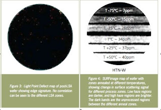
Figure 3 shows a Light Point Defect (LPD) map for the first wafer used in the study. The wafer has typical edge defects, but the LPD map doesn't show noticeable differences among the various anneal process conditions (zones). This implies that any modification to the wafer surface that might have occurred during the laser anneal is below the detection threshold of the defect channel.
However, the SURFimage wafer map (see Fig. 4) shows distinct visual differences among the different process zones on the wafer. The average haze from each process zone was plotted against the LSA temperature.
The figure above shows wide channel haze versus process temperature. It also shows strong correlation between the scattering signal and the anneal temperature.
Previous studies have shown a good correlation between the so-called power spectral density (PSD) and surface roughness as measured by laser scattering. Based on these studies and on this work, the haze results indicate that the wafer surface is modified and roughened by the LSA process. Therefore, the surface roughening increases with LSA temperature.
The authors then reviewed the different zones by SEM to better understand the surface features on the annealed wafer. The results in Fig. 6 show increased surface topography and modification for the zones annealed at higher temperatures.
More annealed wafers (Fig. 7) show similar correlation between LSA temperature and SP2 (?) haze, which shows that this technique is repeatable.
The figure above also shows the raster pattern on the wafer. This technique is also effective at capturing within wafer variations in the surface morphology. A wafer that was annealed at T-75ºC was scanned in high-sensitivity mode on the SURFscan SP2. The SURFimage map (Fig. 8) is effectively able to detect annealing variations within the wafer via changes in the local haze.
The second map shows the wafer binned into low, medium, and high haze regions for ease of view. These results show the ability of SURFimage to provide full-wafer surface information at industrial scale throughputs.
Following this study is planned AFM analysis of the different LSA zones in order to obtain a direct quantitative correlation between the measured surface roughness and haze. Also, the amorphous wafer defectiveness and surface morphology will be also correlated to inline product wafer inspection results. At 45 nm, surface morphology requirements become increasingly strigent. The results here can establish SPC limits for production monitoring of the LSA process.
Conclusion
As ICs shrink to nearly molecular scales, understanding and characterizing the impact of process variations on wafer surface conditions and identifying potential surface damage becomes critical. UV laser scattering technology enables full-wafer surface monitoring with sub-nm vertical resolution and high throughput. This technique can be quite sensitive to small variations in LSA process temperatures that wouldn't be detected by standard defect-monitoring methods; we got ourselves a powerful new tool for process development and monitoring in a fab production environment.


No comments:
Post a Comment